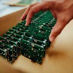
As a manufacturer with years of experience backing our PCB drilling service, we have seen everything that can go wrong during PCB assembly. As a result, we have safeguarded every aspect of the PCB drilling process to ensure these issues do not occur at our facility. Trust our time-tested experts and explore the invaluable methods we employ to deliver the best possible quality to our customers.
Avoiding The Common Pitfalls of PCB Drilling
Don’t: Compromise Hole Location Accuracy
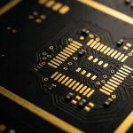
PCB drill “walking” refers to the phenomenon of the drill bit shifting away from the intended hole location during the drilling process. This phenomenon compromises accuracy and increases the risk of breakout in annular rings. When accuracy means everything to PCB design, compromised hole location is one of the more significant issues that can occur during PCB drilling.
Do: Drill Pilot Holes for Proper PCB Drilling
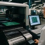
With drill bit walking being such an important issue, how do PCB drill experts address this manufacturing risk? The key to performing PCB drilling is by first implementing a pilot hole before the entire drilling process commences. This pilot drilling procedure is typically carried out by hand but can also be done using a drill press.
Don’t: Allow Roughness Inside the Drilled PCB Hole
Unwanted excess copper, or burrs, is a form of PCB roughness that can occur on PCB surfaces after drilling. After the initial PCB drilling process, there may be roughness leftover within the holes. This roughness can cause several issues in the long run, from barrel cracks to non-uniform copper plating, ultimately leading to lower insulation resistance.
Do: Employ a Deburring Process
Because a build-up of burrs can negatively affect PCB end-product quality and even damage PCB drilling equipment over time, it is crucial to employ a motorized deburring process during any PCB drilling project.
Don’t: Allow Plating Voids During PCB Drilling
To create plated through-holes, the PCB board is drilled, and a copper layer is applied, coating the surface and the walls of the through-holes. The downside of this coating process is that voids in the plating can occur when copper is unevenly applied. These gaps in plating can be detrimental to the quality of the final PCB assembly, as they will block necessary electrical currents.
Do: Utilize Thorough Cleaning Techniques
Defects, such as the previously mentioned uneven copper application, happen when surface contamination and air bubbles are present. These faults can be avoided relatively simply— proper surface cleaning prior to PCB drilling leaves the material in an ideal state for manufacturing.
The Most Important PCB Drilling “Do”: Invest in the Leading Experts
When dealing with a process as complex as PCB drilling, the most crucial step for end-product quality is to entrust the project to a manufacturing team with years of experience under their belts and proven success rates. At SMG, we are proud to be an industry-leading PCB manufacturer, having been committed to prototyping, production, and customization since 1989. Contact our team today if you are interested in PCB drilling services that go above and beyond.