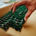
While PCB etching is one of the most basic elements of printed circuit board manufacturing, there are still many complications that compromise the integrity of the final product if PCB etching is performed by a poorly equipped manufacturer. SMG prides itself for not only holding a high standard for quality PCB etching but also for providing guidance to customers looking to better understand this important manufacturing technique. Explore six of the best PCB design practices for quality PCB etch results:
1. PCB Etching Techniques and Tips: Uniform Copper Coating
One of the most important actions that a PCB manufacturer can take to ensure functionality and quality PCB etching results is to create an even copper coating for the printed circuit board base. This uniformity not only allows for less etching fluid to be required during the manufacturing process, it also makes the etching process more predictable and easily workable.
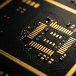
2. PCB Etching Techniques and Tips: Attention to Spacing
Functionality of a printed circuit board is dependent on the spacing of PCB etching processes. Ideally, most boards will maintain 8–10 mils of space between each of the printed circuit board traces. To ensure proper spacing is maintained, manufacturers can employ copper thieving techniques. This typically involves additional copper being poured onto multilayer PCBs.
3. PCB Etching Techniques and Tips: Proper Trace Widths
Similarly to proper spacing, correct trace widths are crucial to producing accurately etched PCBs. Copper thieving is used for maintaining precise trace widths as well as correctly etched spacing. By reinforcing the nominal accuracy of a printed circuit board’s elements, copper thieving will reduce the likelihood of etching errors.
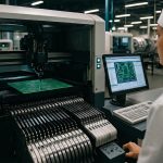
4. PCB Etching Techniques and Tips: Eliminate Byproducts and Debris During the PCB Etching Process
Keeping the printed circuit board’s base clear from debris and contaminants during the etching process is the key to excellent etching results. Beyond maintaining a thoroughly sterilized PCB etching workspace, it is also necessary to continually and quickly remove the byproducts that occur naturally during the PCB etching process.
5. PCB Etching Techniques and Tips: Isolate Critical Traces
Over-etching is one of the most common PCB etching errors. Fortunately, there are techniques that can be employed to avoid this issue. The most common method used to avoid over-etching is the practice of isolating the critical traces of your design, especially as it relates to those PCB elements that are designed in a location that will be surrounded by a smaller amount of copper material.
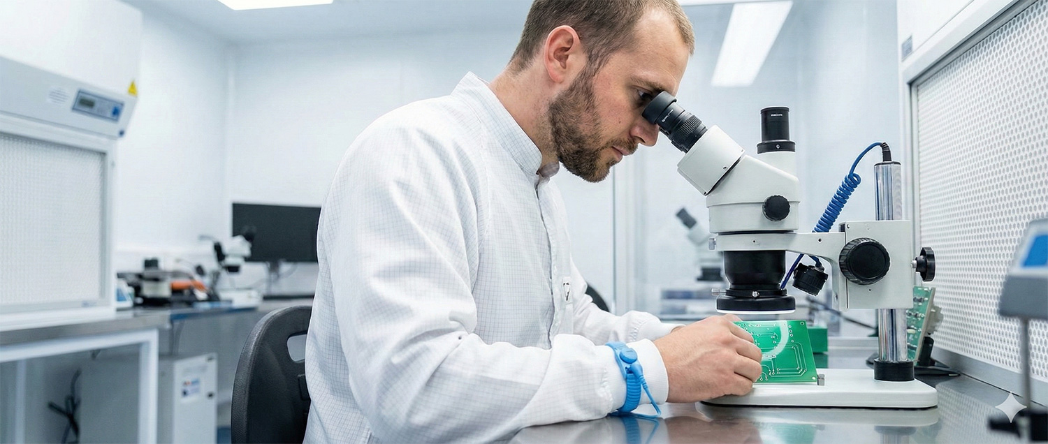
6. PCB Etching Techniques and Tips: Employ First Article Inspection
Finally, once the PCB etching process has been completed, the final best manufacturing practice for PCB etching is to employ first article inspection. During this process, critical traces and impedance measurements are verified to match the intended values. If these measurements do not match, the PCB etching process is reevaluated to understand where the design was compromised. Once it has been fixed, proper PCB etching can be accomplished.