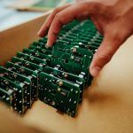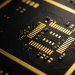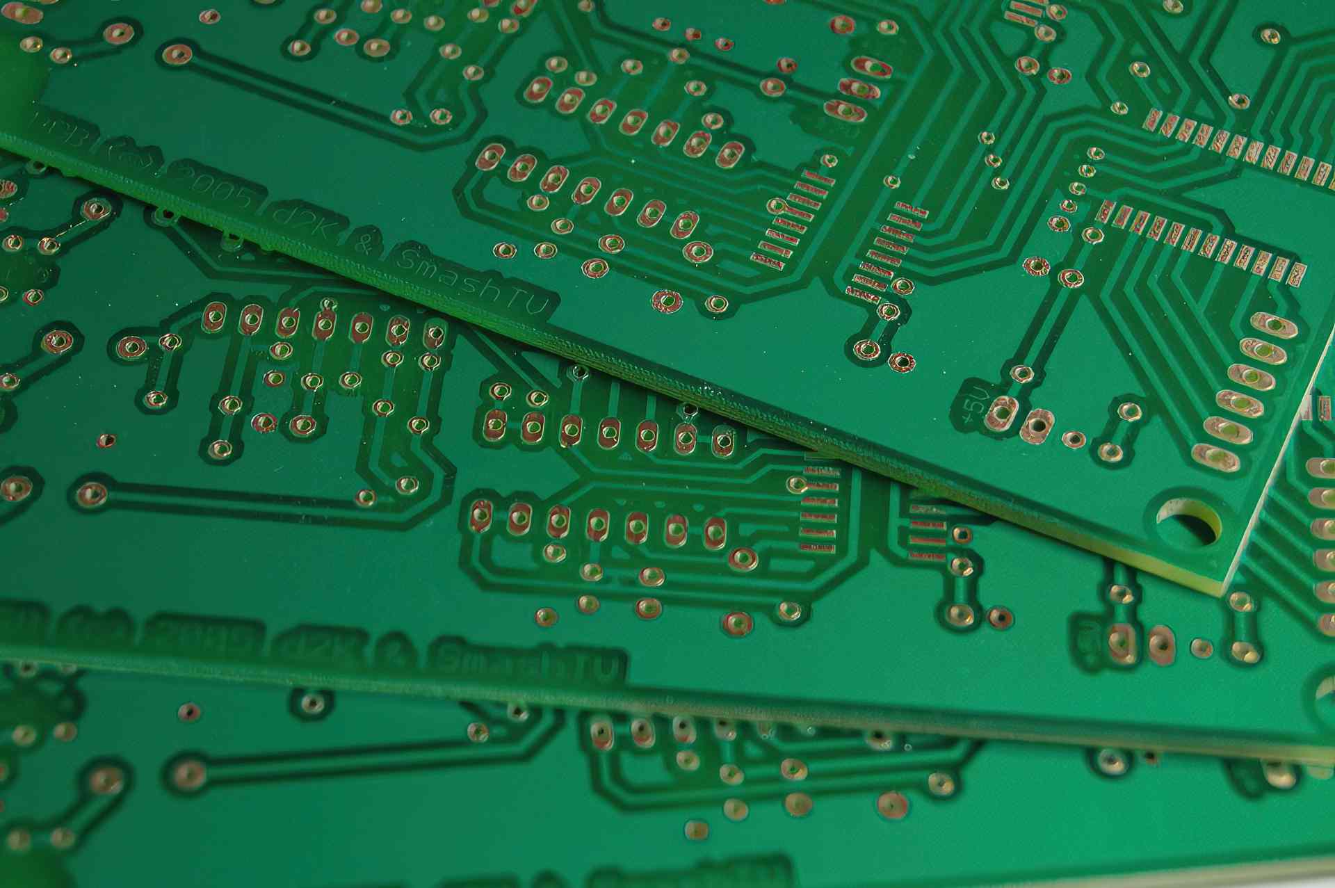
PCB components typically involve exposed copper circuitry, which poses a long-term problem due to copper’s highly corrosive nature. At SMG, we offer a number of finishing services to address this issue and provide the best possible products to our customers. Two of our highly useful finishing processes are electroplating and etching. Learn more about these services below and discover how SMG efficiently provides protective layers as a PCB solutions provider.
What Is Electroplating?
Electroplating is a service in which PCBs are submerged into an electrolyte bath containing metals with an opposite charge to the component. This finishing process bonds those metals to the PCB, resulting in an extra surface layer of protective material. Due to the nature of the electrolyte bath, it is relatively easy to create thicker electroplated layers— our team can simply leave the PCB in the electrically charged solution for a longer period of time. By employing this method of finishing, SMG is able to apply seamless layers of the chosen finishing material to the entire PCB, ensuring uniform depth and coverage for every component.
What Are the Benefits of Electroplating?
There are numerous advantages associated with electroplating. Firstly, the plating process is a considerably cost-effective finishing solution when done correctly, and as a highly-experienced PCB solution provider, SMG helps our customers get the most value out of every finishing service.
Other electroplating advantages include both chemical resistance and corrosion resistance. As mentioned before, an unfinished PCB project involves a great deal of uncovered copper circuitry. Given that copper is highly liable to corrode when exposed even to the open air, it is highly advantageous to invest in a service that will provide long term protection against oxidation.
Lastly, electroplating processes can be advantageous in areas concerning PCB aesthetics. Not every finishing process will offer appealing final appearance results. For example, PCB potting is a finishing process involving placing PCBs within a mold, or pot, in order to be filled with the proper insulating liquid. While potting does its job to increase PCB shock resistance, it is less space-efficient and does not provide the same aesthetically pleasing results that uniform electroplating coating does.
What Is Etching?
Etching is another finishing service for PCBs, providing finer surfaces and high-quality coatings through chemical processes. Much like electroplating, the etching process requires immersion. Using a bath of etching solution, this process provides an even, fine-grained surface. One of the key differences of etching, however, is that during this process the solution bath is typically heated to a predetermined temperature to ensure proper final results.
What Are the Benefits of Etching?
The benefits of etching are similar to electroplating. By imparting a fine-grained etched surface onto PCB components, excess copper circuitry is removed to guard against corrosion— specifically oxidation. Etching is also known for controlling scale build-up, which is particularly advantageous for small-scale PCBs that require high levels of precision. Etching ultimately improves the metal finish of PCB parts by increasing durability and maximizing aesthetic value in the same way that electroplating does, but an additional benefit that is unique to etching is that this process increases resistance to heat damage.